
Nonlinear nano-imaging of interlayer coupling in 2D graphene-semiconductor heterostructures
| REVIEWS AND HIGHLIGHTS | QUANTUM SCIENCE | MOLECULAR AND SOFT-MATTER | ULTRAFAST NANO-OPTICS AND NANOPHOTONICS | MINERALOGY AND GEOCHEMISTRY |
|---|
Wenjin Luo, Renkang Song, Benjamin G. Whetten, Di Huang, Xinbin Cheng, Alexey Belyanin, Tao Jiang, Markus B. Raschke
Small, 2024, 2307345 (2024).
DOI PDF SI
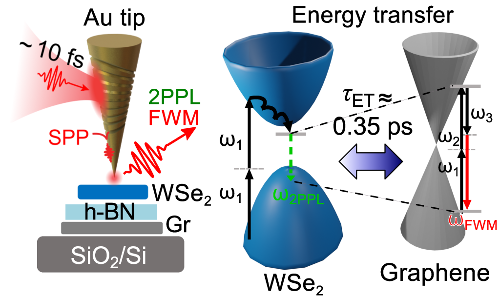
The emergent electronic, spin, and other quantum properties of 2D heterostructures of graphene and transition metal dichalcogenides are controlled by the underlying interlayer coupling and associated charge and energy transfer dynamics. However, these processes are sensitive to interlayer distance and crystallographic orientation, which are in turn affected by defects, grain boundaries, or other nanoscale heterogeneities. This obfuscates the distinction between interlayer charge and energy transfer. Here, nanoscale imaging in coherent four-wave mixing (FWM) and incoherent two-photon photoluminescence (2PPL) is combined with a tip distance-dependent coupled rate equation model to resolve the underlying intra- and inter-layer dynamics while avoiding the influence of structural heterogeneities in mono- to multi-layer graphene/WSe2 heterostructures. With selective insertion of hBN spacer layers, it is shown that energy, as opposed to charge transfer, dominates the interlayer-coupled optical response. From the distinct nano-FWM and -2PPL tip-sample distance-dependent modification of interlayer and intralayer relaxation by tip-induced enhancement and quenching, an interlayer energy transfer time of τET≈(0.35−0.15+0.65) ps consistent with recent reports is derived. As a local probe technique, this approach highlights the ability to determine intrinsic sample properties even in the presence of large sample heterogeneity.