
Inducing and probing localized excitons in atomically thin semiconductors via tip-enhanced cavity-spectroscopy
| Reviews and Highlights | Quantum Science | Molecular and Soft-matter | Ultrafast Nano-optics and Nanophotonics | Mineralogy and Geochemistry |
|---|
Hyeongwoo Lee, Inki Kim, Chulho Park, Mingu Kang, Jinseong Choi, Kwang-Yong Jeong, Jungho Mun, Yeseul Kim, Jeonghoon Park, Markus B. Raschke, Hong-Gyu Park, Mun Seok Jeong, Junsuk Rho, and Kyoung-Duck Park
Adv. Funct. Mater. 31, 2102893 (2021).
DOI PDF SI
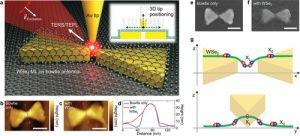 In atomically thin semiconductors, localized exciton (XL) coupled to light provides a new class of optical sources for potential applications in quantum communication. However, in most studies, XL photoluminescence (PL) from crystal defects has mainly been observed in cryogenic conditions because of their sub-wavelength emission region and low quantum yield at room temperature. Hybrid-modality of cavity-spectroscopy to induce and probe the XL emissions at the nanoscale in atomically thin semiconductors is presented. By placing a WSe2 monolayer on the two extremely sharp Au tips in a bowtie antenna with a radius of curvature of <1 nm, tensile strain of ≈0.3% is effectively induced in a <30 nm region to create robust XL states. The Au tip then approaches the strained crystal region to enhance the XL emissions and probe them with tip-enhanced photoluminescence (TEPL) spectroscopy at room temperature. Through this triple-sharp-tips cavity-spectroscopy with <15 nm spatial resolution, TEPL enhancement as high as ≈4.0 × 10⁴ by the Purcell effect is achieved, and peak energy shifts of XL up to ≈40 meV are observed. This approach combining nano-cavity and -spectroscopy provides a systematic way to induce and probe the radiative emission of localized excitons in 2D semiconductors offering new strategies for dynamic quantum nano-optical devices.