
Nanoimaging of electronic heterogeneity in Bi2Se3 and Sb2Te3 nanocrystals
| Reviews and Highlights | Quantum Science | Molecular and Soft-matter | Ultrafast Nano-optics and Nanophotonics | Mineralogy and Geochemistry |
|---|
Xiaowei W. Lu, Omar Khatib, Xutao T. Du, Jiahua H. Duan, Wei Wei, Xianli L. Liu, Hans A. Bechtel, Fausto D’Apuzzo, Mingtao T. Yan, Alexander Buyanin, Quiang Fu, Jianing N. Chen, Miquel Salmeron, Jie Zeng, Markus B. Raschke, Peng Jiang, and Xinhe H. Bao
Adv. Electron. Mater. 4, 1700377 (2017).
DOI PDF SI
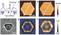
Topological insulators (TIs) are quantum materials with topologically protected surface states surrounding an insulating bulk. However, defect-induced bulk conduction often dominates transport properties in most TI materials, obscuring the Dirac surface states. In order to realize intrinsic topological insulating properties, it is thus of great significance to identify the spatial distribution of defects, understand their formation mechanism, and finally control or eliminate their influence. Here, the electronic heterogeneity in polyol-synthesized Bi2Se3 and chemical vapor deposition-grown Sb2Te3 nanocrystals is systematically investigated by multimodal atomic-to-mesoscale resolution imaging. In particular, by combining the Drude response sensitivity of infrared scattering-type scanning near-field optical microscopy with the work-function specificity of mirror electron microscopy, characteristic mesoscopic patterns are identified, which are related to carrier concentration modulation originating from the formation of defects during the crystal growth process. This correlative imaging and modeling approach thus provides the desired guidance for optimization of growth parameters, crucial for preparing TI nanomaterials to display their intrinsic exotic Dirac properties.